|
|
||||||
|
|
|
|
Download | |||
Diamond Version 5 User Manual: Automatic, assisted, and manual picture creationDefinition and Application of "Design Schemes"Design schemes are some kind of style sheets with design and viewing settings to be applied to structure pictures
Design schemes in brief:
Previous article: Building schemes
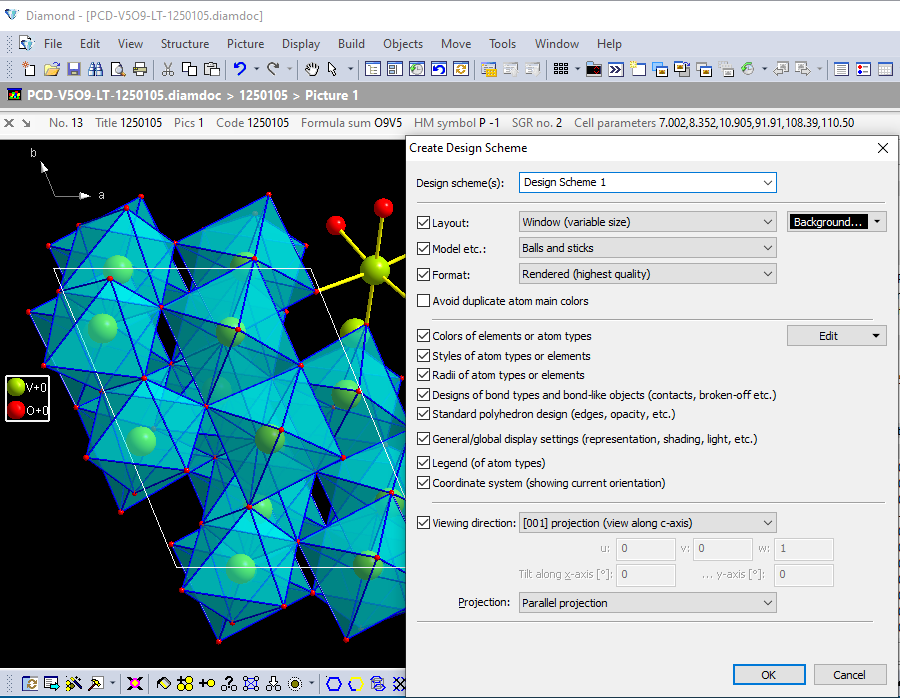
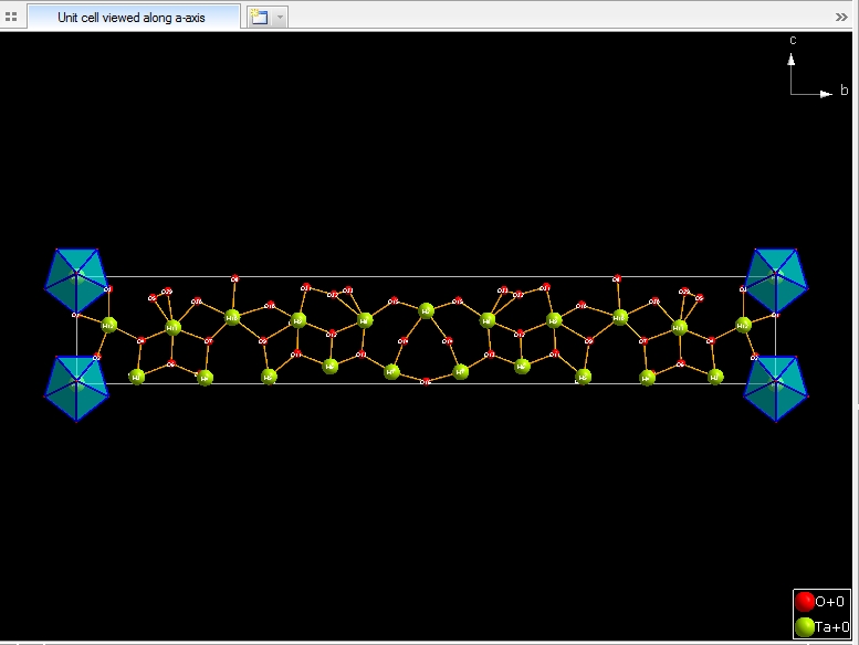
Definition of a design scheme You find the commands that deal with design schemes in the corresponding submenu of the Display menu. The first command Create Design Scheme From Picture... initializes a design scheme from the current picture settings -- from layout, model, rendering or not, across the atom, bond etc. designs up to the viewing direction. Use the checkboxes to decide what the new design scheme may change when applied later. For instance, you can create a design scheme that only reflects the atom (type) designs. So you can easily change current atoms' designs to have different colors, ellipsoid styles, etc. The second command Create Design Scheme From Selection... (introduced in version 5.1) does not access the global picture settings but the designs of the atoms that are currently marked as selected as well as the designs of the selected bonds, contacts, and H-bonds and the designs (of faces and edges) of the currently selected polyhedra. This is well suited to create design schemes for special building units, e.g. inorganic units with complex polyhedra or molecular fragments. We show the definition and application of design schemes in the following scenarios. Scenarios #1 through #3 work with global picture settings, while scenario #4 demonstrates how to define a design scheme from the atoms and bonds of a selected molecular fragment that can be used as organic linker in Metal Organic Frameworks (MOF). Scenario 1: Defining a design scheme and applying to another structureThe following screenshot shows the Design Scheme dialog. Open the sample file "PCD-V5O9-LT-1250105.diamdoc", which contains one picture with a unit cell viewed along c-axis and with semi-transparent coordination polyhedra around all V atoms.
Defining the design scheme
In the next section you find the basic settings with options that you already know
from the "Picture Creation Assistant", concerning:
The third section enables storing of individual settings concerning the picture
design of the current picture - provided that the corresponding checkmark is set.
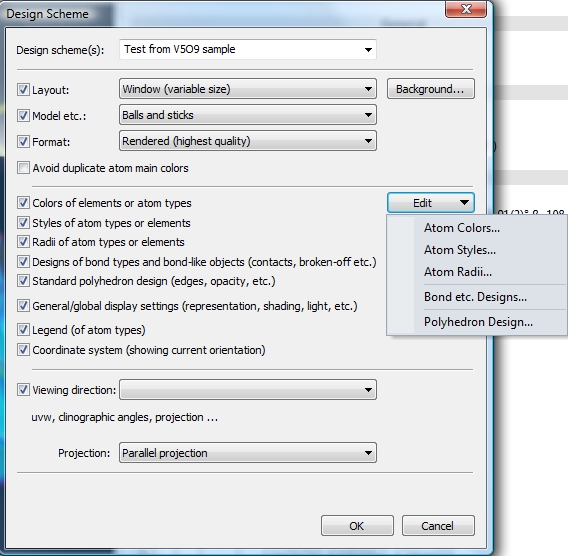
These are: The fourth section is for viewing direction and projection, and has already been available in "Picture Creation Assistant" since Diamond version 3. Before we save this design scheme as new design scheme with the title "Test from V5O9 sample" in the Windows Registry, we will point you to some additional possibilities to make changes - for instance in atom, bond, and polyhedron designs. Push the Edit menu button (in the Design Scheme dialog), which opens a menu with commands to edit atoms' (better: the atom types' or elements') colors, styles, and/or radii as well as properties of bonds and bond-like objects and polyhedra. Note: Some screenshots in this article have been made with version 4 of Diamond.
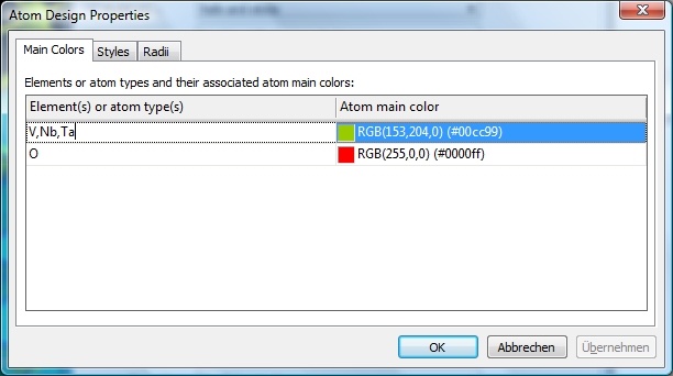
Commands Atom Colors..., Atom Styles..., and Atom Radii... open the Atom Design Properties dialog, which begins with two rows, one for "V+0" and one for "O+0". If you want not only V but e.g. also Nb and Ta to become lime green when assigning the design scheme "Test from V5O9 sample", you can edit the element (or atom type) in the corresponding table cell. The same works for atom types' (or elements') styles and radii on the other two pages Styles and Radii, rsp. (here not depicted).
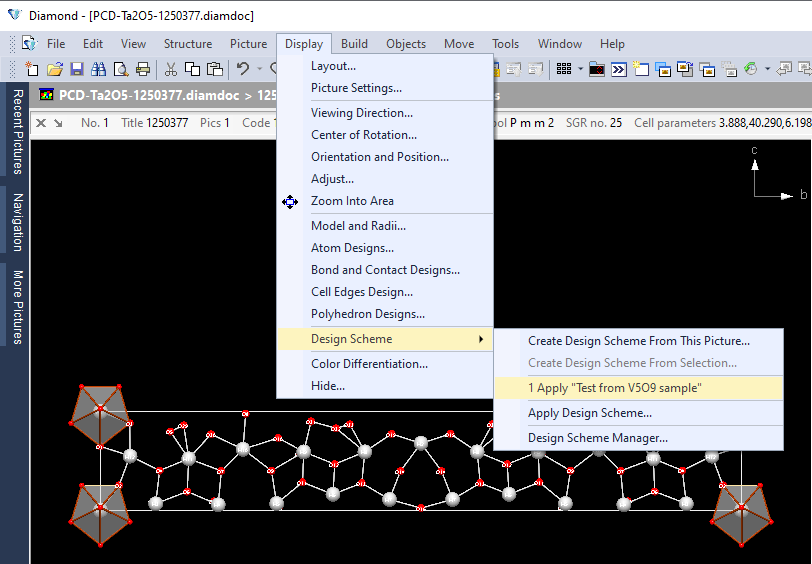
Application of a design scheme
The Ta atoms and the bonds are light gray (color delivered from Diamond export from Pearson's Crystal Data) and turn -- after application of the design scheme -- into lime green (Ta) and yellow (bonds), rsp. (To change the coordination polyhedra, we have to call Display -> Polyhedron Designs..., ensure that the Update existing polyhedra checkmark is set and confirm with OK.)
"Apply Design Scheme" dialog
Two ways of creating a design scheme (2) Use the "Auto Picture Creator" to approach your preferred design by changing settings for Layout, Model etc., and Format in the Picture design category, and then run Create Design Scheme dialog like described under (1).
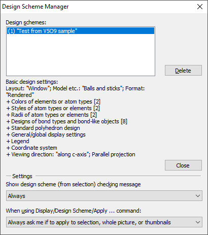
Design Scheme Manager The Settings in the lower part of the dialog define, if and how far you will be prompted, if there are ambiguities when creating a design scheme from selected atoms etc. and where to apply a design scheme, if there are currently selected objects in the structure picture.
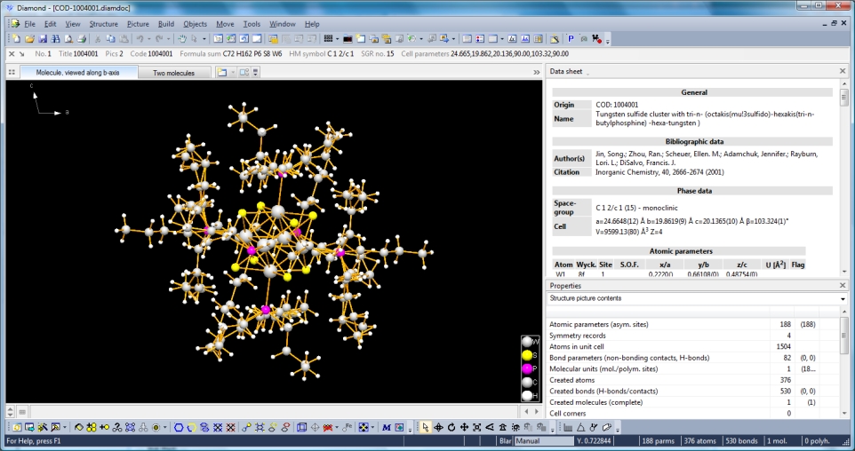
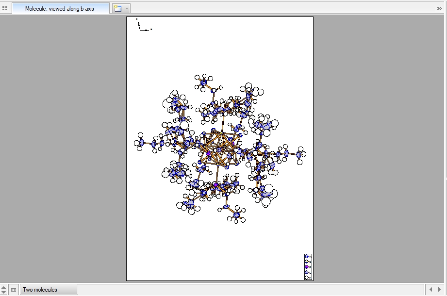
Scenario 2: Quick definition and application of a design schemeMake your structure picture settings (a rendered colorful screen plot or an ORTEP-like ellipsoid sketch on white paper) along with the designs of atom (groups, sites), bonds, polyhedra, etc. -- and simply call Create Design Scheme to create a design scheme from these current picture settings and save it under a title, so you can access this scheme whenever you later want to quickly re-design a picture from another structure. The following example shows how to quickly re-design a rendered color picture to a flat color-line ellipsoid sketch on a white A4 page. After loading sample file "COD-1004001.diamdoc", which begins with picture "Molecule, viewed along b-axis":
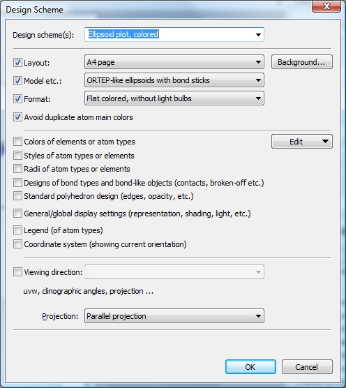
The default or current setting is "window layout", "ball-and-stick model" and "rendered". We run the command Display -> Design Schemes -> Create Design Scheme... and make the following settings in order to get a design scheme for an A4 printout page, thermal ellipsoids, and flat color line representation:
We call this design scheme "Ellipsoid plot, colored". Ensure that the checkmarks are set in Layout, Model etc., Format and Avoid duplicate atom main colors and the other checkmarks are cleared. Then store this design scheme with OK. Application of a design scheme that has been created previously titled "Ellipsoid plot, colored" will now be applied to the structure picture "Molecule, viewed along b-axis" resulting in this page layout with white background and black outlined bonds and atoms in ellipsoid representation:
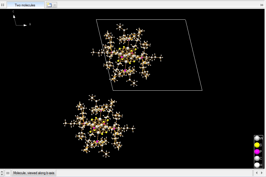
Well, this could be easier done with a function like Picture -> Picture Creation Assistant (leaving picture building and viewing direction unchanged but setting the options on the picture design page as stated above. But we want to apply the design scheme now to another picture, and maybe later to more pictures, whenever we want to have a flat-looking color printout in A4 size. Switching to the second picture in the document, entitled with "Two molecules" ...
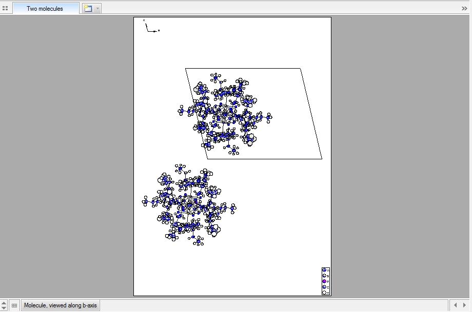
... applying design scheme "Ellipsoid plot, colored" leads to:
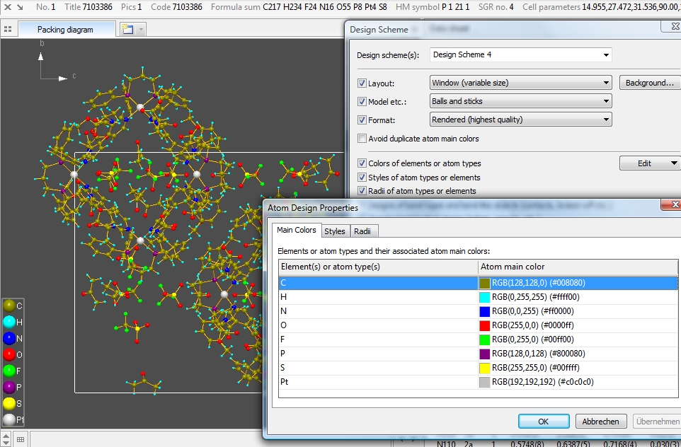
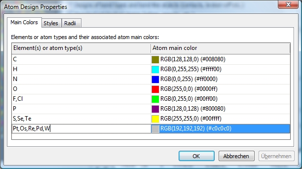
When using the "Auto Picture Creator", the simplest way is to choose the design scheme from the "Scheme" combobox in the "Picture design" section of the Auto Picture Creator. Other ways -- if you prefer manual changes at your structure picture -- is to choose the appropriate design scheme from the Design Schemes sub-menu in the Display menu. When running Apply Design Scheme from a Design Scheme dialog, you have additional choices which fields of the scheme to apply, e.g. just the atom and bond desings but leaving rendering options and background color settings unchanged. Scenario 3: Using design schemes to create atom color, style and radii resourcesThe most convenient way to create a design scheme is from an existing structure picture. The scenario 3 part of the article shows you how to derive a set of resources for atom main colors, atom styles, and radii. Since there are a lot of settings that affect the appearance of a structure picture, such as layout, background color, rendered or flat, enlargement factor etc., the easiest way to create a design scheme is to build a structure picture, and then to call the Create Design Scheme command from the Design Schemes sub-menu in the Display menu. The disadvantage is that you have just a small subset of different elements or atom types in your structure. If you take the design scheme created from that structure and apply it to another structure but with different elements, these other elements' colors (and styles and radii) would not be affected by the design scheme. The screen shot below (sample "COD-7103386.diamdoc") shows the design scheme settings dialog and the set of atom main colors generated from that structure - here just Pt, S, P, N, O, F, C, and H.
To extend the definition of atom main colors, atom styles, and radii for ball and space-filling representation to other elements than just Pt, S, P, N, O, F, C, and H,, run Edit in the Design Scheme dialog. Enter the element symbols in the corresponding row of the Elements or atom types column and confirm with OK, example below:
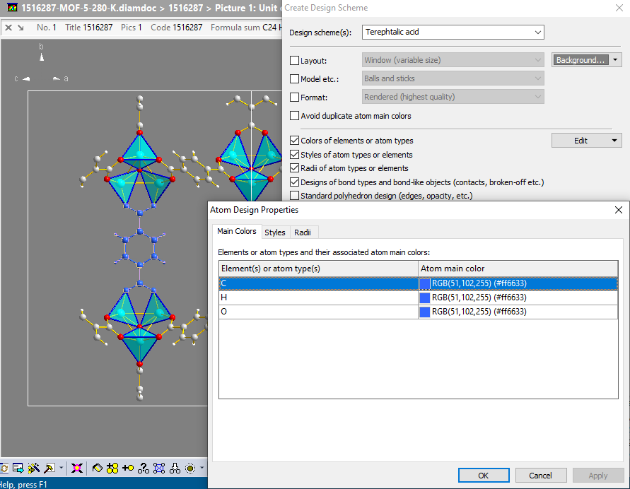
Give this design scheme an appropriate title and assign it later to structures containing similar elements, e.g. Cl instead of F, or Se or Te instead of S, etc. Scenario 4: Creating design schemes for organic linkersThe best way to create design schemes for special building units like complex polyhedra or molecular fragments that are part of a complex (metal-)organic framework is to start from a set of selected atoms, bonds, and if necessary polyhedra. Here we show how to define a design scheme for terephtalic acid, which is an organic linker in many metal-organic frameworks (MOF). Creating the design scheme Checking the main colors of the elements of the selected atoms (C, H, O) by using the Edit dropdown button shows they use the same color in the design scheme:
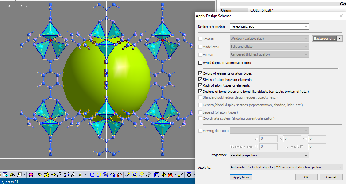
We close the Create Design Scheme dialog with OK. The design scheme "Terephtalic acid" will now be available through the Design Scheme Manager and the Apply Design Scheme dialog. Applying the design scheme This will prompt you if you want to apply the selected design scheme (here: "Terephtalic acid") to the current selection or to the whole picture. Choose "Yes". An alternative is to choose the command Apply Design Scheme... where you can choose your design scheme from the Design schemes dropdown list at the top of the dialog and choose your target option from the Apply to dropdown list at the bottom of the dialog. The advantage is that you can disable unwanted properties when applying a design scheme. As you see, some of the properties are greyed out. This is because you have created the design scheme from selection rather than from the whole picture and thus these general properties have not been included:
Note: Design schemes created from selected atoms, bonds, and/or polyhedra are not limited to the structural unit where they have been created from. So you can apply a design scheme such as "Terephtalic acid" to all organic linkers (or molecular or polymeric units in general) containing C, H, and O.
Previous article: Building schemes
References: |
|
Page last modified October 22, 2024. Copyright © 2024 Crystal Impact GbR. All rights reserved. Contact Webmaster |